In our always-on world, electrons are racing through wires, chips, and screens every second, lighting our homes and feeding hungry data centers. That invisible traffic has a cost in rising electricity demand and more pressure on power grids. Now physicists say they have taken a step that could, one day, help squeeze more work out of every electron.
For the first time, an international team led by MIT has measured the “shape” of electrons moving through a solid crystal, turning a long-standing theory into hard experimental data.
Seeing electrons as shapes
Using a technique known as angle resolved photoemission spectroscopy, or ARPES, the researchers mapped the quantum geometry of electrons in a material known as a kagome metal. This geometry describes how an electron’s wave-like nature spreads out and twists inside the crystal instead of treating the particle as a simple point. The work, reported in Nature Physics in late 2024, provides the first direct reconstruction of that geometry in a real solid.
Riccardo Comin, the MIT physicist who led the study, said the results “open new avenues for understanding and manipulating the quantum properties of materials.” He also described the new method as “a blueprint for obtaining some completely new information that could not be obtained before.”
In plain language, the team is looking at the shapes traced out by electron waves. A very simple wave function can resemble a smooth bubble.More exotic wave functions behave more like loops with a twist, similar to a Möbius strip from art and math. Many quantum materials are built from these more complicated patterns, and those patterns can give rise to unusual effects such as superconductivity and strange magnetic behavior.
From exotic metals to everyday devices
The experiments focused on a kagome metal, a family of compounds where atoms sit in a pattern of corner-sharing triangles that resembles traditional Japanese basket weaving. That geometry forces electrons to move in unusual ways and can create flat energy bands, where particles crowd into the same energy and interact very strongly.
Studies over the past few years have shown that kagome metals can host superconductivity, charge order, and other collective phases that are especially sensitive to quantum geometry.
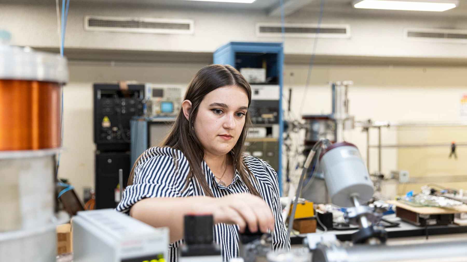
In ARPES, intense light shines on the crystal and knocks electrons out from its surface. Detectors capture the energy, direction, and spin of those escaping electrons. From that set of fingerprints, the team can reconstruct how electrons were arranged and moving inside the material, including the subtle twists that define their quantum shape.
It is a demanding approach that relies on powerful light sources and highly stable instruments, but it gives a kind of three-dimensional map of electron behavior that was out of reach until now.
Why this matters for a warming planet
At first glance, all this talk of wave functions and kagome lattices may feel far from everyday worries like the size of your electric bill or that sticky summer heat when air conditioners and servers strain the grid.
Yet the geometry measured in this work is directly tied to how easily electrons flow, how strongly they interact, and how much energy they lose as heat. Researchers see quantum geometry as a key ingredient in designing future superconductors and ultra-efficient electronic components that move charge with minimal resistance.
That kind of efficiency is not just a lab curiosity. The information and communications technology sector already uses about 4% of global electricity. Data centers alone are estimated to consume around 1 to 1.5% of the world’s power, and analyses from the International Energy Agency (IEA) suggest that their demand could roughly double by 2030 as artificial intelligence and cloud services expand.
Every improvement in how electrons move through chips, memory, and interconnects can, in principle, help slow that growth.
The new measurements do not deliver that greener hardware overnight. What they do is give scientists a practical recipe to read and eventually engineer the quantum geometry that underpins many of the most promising energy-saving materials.
The same ideas that govern electrons in kagome metals also appear in devices for quantum sensing, where ultra precise measurements of current and magnetic fields could help monitor power lines, reduce losses, and support the integration of more solar and wind energy into the grid.
One tiny particle, many future paths
Researchers now plan to apply this ARPES-based blueprint to a wider range of crystals, building a catalog of quantum geometries and learning how to tune them. Some scientists describe this effort as part of a second quantum revolution, focused not only on understanding quantum effects but on using them deliberately in devices.
In practical terms, that means future materials for quantum computers, low-loss power electronics, or ultra-sensitive sensors may be designed with their electron “shapes” in mind rather than discovered by trial and error.
The journey from this fundamental result to cooler data centers or lighter grid emissions will be long and full of engineering hurdles. Still, by finally seeing how electrons curve and twist inside solids, scientists have gained a tool that could, to a large extent, change how we think about the building blocks of a more sustainable digital world.
The study was published in Nature.


