A tiny redesign beneath an ultrathin superconductor may point toward a new generation of far more efficient electronics. Researchers in Sweden found that shaping the surface under a superconducting material helped it keep its special properties at higher temperatures and under stronger magnetic fields.
That matters because superconductors can carry electric current without electrical resistance, meaning they do not waste energy as heat in the usual way. This is not a room-temperature superconductor ready for your laptop next year, but it does offer a new route around one of the toughest barriers in modern physics.
Why superconductors matter
Most electronics lose some energy as heat. You can feel it in a warm phone, a hot laptop charger, or the cooling fans that keep data centers from turning into ovens.
Superconductors work differently. When they are in their superconducting state, electric current can move through them without resistance, which could make some power systems, quantum devices, and electronic components much more efficient.
Digital devices, data centers, and information and communication technology networks now account for roughly 6 to 12 percent of global electricity use, according to figures cited by Chalmers University of Technology. That is why even a small gain in efficiency could matter at the scale of the electric bill, the power grid, and the internet itself.
The old roadblock
The catch has always been real-life application. Many superconductors need extremely cold conditions, often around 328 degrees Fahrenheit below zero, and keeping materials that cold takes complex and energy-thirsty equipment.
Strong magnetic fields are another problem. They can weaken superconductivity or wipe it out completely, which is a serious issue because advanced electronics and many quantum technologies often involve magnetic fields.
So the question is simple. Can scientists make superconductors that stay useful when conditions get tougher? That is where the new surface design comes in.
The surface did the work
The team studied a copper-oxide material from a family known as cuprates. These materials are already well-known among physicists because they can become superconducting at relatively higher temperatures than many older superconductors.
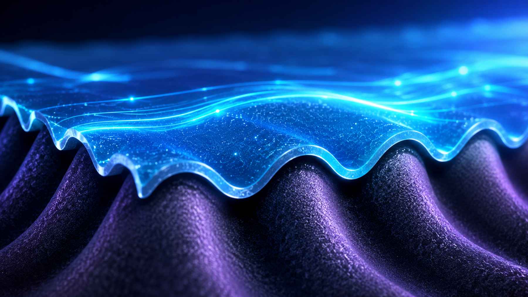
Instead of changing the chemistry of the superconductor itself, the researchers changed the surface it was grown on. Think of it like preparing the ground before laying tile. The pattern underneath can influence how everything settles on top.
The superconducting layer was extremely thin, far less than one millionth the thickness of a human hair. Before adding it, the team treated the supporting surface in a vacuum at high temperature, creating tiny ridges and valleys that guided how the atoms arranged themselves.
A tiny pattern, a big effect
That nanoscale landscape changed the meeting point between the support layer and the superconductor. At that boundary, the electrons began behaving with a preferred direction, which helped strengthen the superconducting state.
In the study, thinner films grown on the specially shaped surface began superconducting at temperatures more than 27 degrees Fahrenheit higher than thicker comparison films. They also held up better under very strong magnetic fields, a key test for future electronic and quantum applications.
Floriana Lombardi, professor of quantum device physics at Chalmers and lead author of the work, said the finding shows that “very small changes at the nanoscale can have decisive effects.” In practical terms, a barely visible surface change altered how the entire material behaved.
A different route to better materials
For years, many researchers have tried to improve superconductors by changing their chemical recipe. That approach has produced progress, but it can also be difficult, especially once complex materials have already been made.
This work suggests another path. Rather than searching only for brand-new materials, scientists may be able to boost performance by engineering the surface beneath them, a strategy Lombardi described as “sculpting the substrate.”
Could this help bring superconductors closer to everyday use? To a large extent, that depends on whether the method can be repeated, scaled up, and adapted to devices outside the lab. Still, the idea is promising because it changes where researchers look for improvements.
Who was behind the study
The research was led by scientists at Chalmers University of Technology, with Eric Wahlberg of RISE Research Institutes of Sweden among the key researchers involved. Riccardo Arpaia, Debmalya Chakraborty, Alexei Kalaboukhov, David Vignolles, Cyril Proust, Annica M. Black-Schaffer, Thilo Bauch, Götz Seibold, and Lombardi are listed among the authors of the paper.
The project also involved partners from Ca’ Foscari University of Venice, Birla Institute of Technology and Science Pilani, Indian Institute of Science Education and Research, Uppsala University, Université Grenoble Alpes, Université de Toulouse, INSA-T, and BTU Cottbus-Senftenberg.
Part of the work was carried out at Myfab Chalmers, and support came from the Swedish Research Council, the Knut and Alice Wallenberg Foundation, the European Union through an EIC Pathfinder grant, and the Deutsche Forschungsgemeinschaft.
What comes next
This is still research, not a finished technology. Scientists will need to test whether the same design principle works in other superconducting materials, whether it survives real manufacturing conditions, and whether it can be built into useful components.
But the message is clear enough. Sometimes the future of electronics does not depend only on inventing a new material. Sometimes it starts with reshaping the surface beneath it.
The official study has been published in Nature Communications.